Samsung expected to show cutting-edge 3-nm chip to Biden during Pyeongtaek campus visit

SEOUL, May 19 (Yonhap) -- Samsung Electronics Co. is expected to showcase one of its most advanced chipmaking technologies to U.S. President Joe Biden when he visits its Pyeongtaek campus this week, sources said Thursday.
Biden is set to arrive in Seoul Friday on his first visit to the country since taking office, and only 10 days after South Korea's new President Yoon Suk-yeol took office.
His three-day visit to South Korea will start with a tour of Samsung's Pyeongtaek complex, the world's largest semiconductor facility, located some 70 kilometers south of Seoul.
Samsung Electronics Vice Chairman Lee Jae-yong is said to provide a personal tour of the massive complex.
Samsung is expected to show its next-generation 3-nanometer (nm) semiconductor built on the Gate-All-Around (GAA) technology, which Samsung will mass produce within the next couple of months.
"Samsung could show a 3-nm chip to Biden to emphasize its foundry prowess over Taiwan's TSMC," an official with the knowledge of Samsung's advanced chip technology said.
The GAA process allows for an up to 35-percent decrease in size while providing 30 percent higher performance, or 50 percent lower power consumption, compared to the 5nm process, according to Samsung.
Samsung, the world's largest memory chip maker and second largest foundry player, has said its 2nm process node was in the early stages of development with mass production in 2025.
TSMC, the world's largest contract chip manufacturer, and Samsung have been in fierce competition to outperform each other by bringing the 3-nm chips to the mass market.
According to industry tracker TrendForce, TSMC took up 52.1 percent of the global foundry market, followed by Samsung with 18.3 percent, in the fourth quarter of last year.
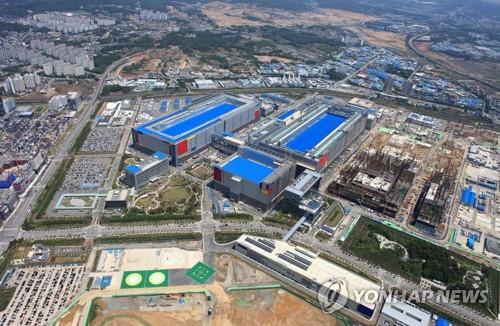
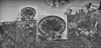
The photo provided by Samsung Electronics Co. shows its semiconductor complex in Pyeongtaek, some 70 kilometers south of Seoul. (PHOTO NOT FOR SALE) (Yonhap)
jaeyeon.woo@yna.co.kr
(END)
-
 Defense chief says N. Korea's hypersonic missile 'unsuccessful' in last-stage glide flight
 -
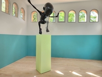
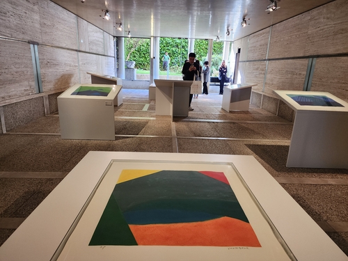
 Overdue debut of Korean abstract art pioneer Yoo Young-kuk at Venice Biennale
 -
 Relax, immerse yourself in scents at Venice Biennale's Korean Pavilion
 -
 N. Korea has capability to genetically engineer biological military products: U.S. report
 -
 Leader of new minor party proposes talks with Yoon


-
 Overdue debut of Korean abstract art pioneer Yoo Young-kuk at Venice Biennale
 -
 Relax, immerse yourself in scents at Venice Biennale's Korean Pavilion
 -
 Defense chief says N. Korea's hypersonic missile 'unsuccessful' in last-stage glide flight
 -
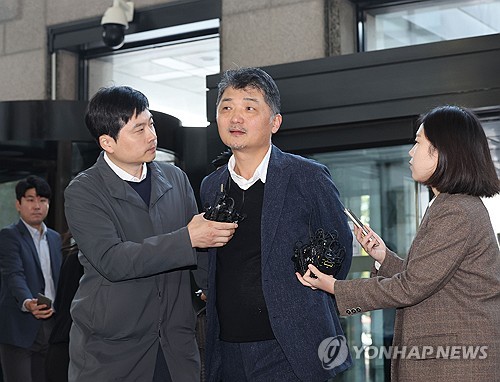 Questioning necessary for Kakao founder for suspected stock rigging: prosecution
 -
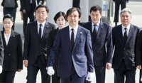
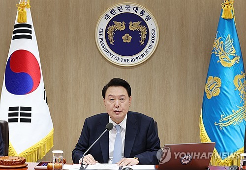 (LEAD) Yoon vows to improve communication with people after election defeat


-
 Facebook page unveils photos of BTS member V in counter-terrorism unit gear
 -
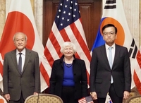 (4th LD) Finance chiefs of S. Korea, U.S., Japan recognize 'serious' concerns over 'sharp' won, yen depreciation
 -
 S. Korea to provide US$200 million in humanitarian aid to Ukraine this year
 -
 (2nd LD) N. Korea removes street lamps along inter-Korean roads
 -
 Gov't likely to accept university chiefs' request to lower med school enrollment quota